Why GaN vs Silicon Matters in Modern Power Adapters
Gallium Nitride (GaN) technology represents a major shift in power electronics, fundamentally changing how chargers and power adapters are designed. Compared to traditional silicon-based chargers, GaN enables significantly higher efficiency, reduced heat generation, and much smaller form factors.
In practical terms, this means modern GaN chargers can deliver the same or higher power output while being smaller, cooler, and more energy efficient than conventional silicon-based alternatives.
At a system level, GaN devices improve overall conversion efficiency by approximately 10%, while reducing physical size by nearly half in many power adapter designs. This is why GaN has rapidly become the preferred technology in high-performance USB-C chargers, laptop adapters, and compact industrial power supplies.
This article explains in detail:
- What GaN technology is and how it works
- Key differences between GaN and silicon chargers
- Why GaN enables higher efficiency and faster charging
- Real-world applications and design advantages
What is GaN Technology in Chargers?
Gallium Nitride (GaN) is a wide bandgap semiconductor material used as a replacement for silicon in power switching devices. In power adapters, GaN is used in transistors that regulate voltage conversion and energy transfer.
Compared to silicon, GaN has superior electrical properties:
- Higher electron mobility
- Higher breakdown voltage capability
- Lower switching and conduction losses
- Faster switching speed at high frequencies
These characteristics allow GaN-based chargers to operate more efficiently while generating less heat, even under high power loads.
In simple terms, GaN enables power adapters to “switch electricity” faster and more efficiently, which directly leads to smaller size and higher performance.
Quick Comparison: GaN vs Silicon Chargers
| Feature | GaN Chargers | Silicon Chargers |
|---|---|---|
| Energy Efficiency | Higher (up to ~95%) | Lower (~80–87%) |
| Heat Generation | Low | High |
| Switching Speed | Very High (MHz range) | Lower (kHz range) |
| Size / Form Factor | Compact | Larger and bulkier |
| Power Density | Very High | Limited |
| Lifespan | Longer (lower thermal stress) | Shorter (heat degradation) |
This table summarizes why GaN is increasingly replacing silicon in modern power adapter design, especially for high-wattage and portable applications.
How GaN Technology Works in Power Adapters
The core advantage of GaN lies in its ability to switch electrical signals at extremely high speeds with minimal energy loss.
High-Frequency Switching Capability
Traditional silicon MOSFETs typically operate at switching frequencies in the range of a few hundred kilohertz. In contrast, GaN devices can operate at frequencies reaching several megahertz.
At the transistor level:
- Silicon switching time: ~20–50 nanoseconds
- GaN switching time: ~1–2 nanoseconds
This 10× improvement in switching speed significantly reduces energy loss during each transition cycle.
Higher switching frequency also allows engineers to reduce the size of passive components such as:
- Transformers
- Inductors
- Capacitors
This is one of the main reasons GaN chargers are dramatically smaller.
Reduced Switching Loss and Conduction Loss
In silicon-based devices, energy is lost during:
- Turn-on transition (current overlaps voltage)
- Turn-off transition (delayed current interruption)
- Body diode reverse recovery
GaN devices eliminate or reduce many of these losses due to:
- No traditional body diode behavior
- Faster transition between states
- Lower Rds(on) resistance
As a result, less energy is wasted as heat, improving overall conversion efficiency.
Dead Time Optimization
“Dead time” refers to the brief delay between switching cycles designed to prevent short circuits.
In silicon systems:
- Longer dead time is required
- More energy is lost during transitions
In GaN systems:
- Ultra-fast switching reduces required dead time
- More energy is delivered directly to the load
- Overall efficiency improves
This is particularly important in high-frequency DC-DC converters used in fast chargers and USB-C Power Delivery systems.
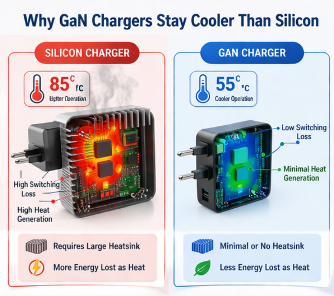
Why GaN Chargers Stay Cooler Than Silicon
Heat has always been the archenemy of electronic components. Traditional silicon chargers struggle with this challenge, often becoming noticeably warm during operation. This thermal issue stems from fundamental limitations in silicon’s electrical properties. However, GaN technology chargers address this problem at its source.
Lower conduction and switching losses in GaN
The superior thermal performance of GaN begins with its exceptional electrical characteristics. Unlike silicon, GaN offers significantly lower resistance when conducting electricity – a property known as Rds(on). For any given breakdown voltage, GaN devices provide the lowest Rds(on) values compared to both silicon and silicon carbide materials. This directly translates to reduced conduction losses when the transistor is turned on.
Switching losses present another major source of heat generation in chargers. These occur during the brief moments when transistors transition between on and off states. GaN excels here too, as its transistors can switch at considerably faster speeds than silicon counterparts. During the turn-on process, current in silicon transistors begins flowing before the drain-to-source voltage drops, creating substantial energy loss. GaN significantly reduces these losses through rapid switching capabilities.
Notably, GaN transistors lack the body diode found in silicon MOSFETs. Consequently, current that would normally flow through the inefficient body diode instead passes through GaN’s low-resistance pathway. This characteristic results in almost zero reverse recovery loss, further minimizing heat generation.
Heat in power adapters is mainly caused by electrical losses during conversion. Since GaN reduces both conduction and switching losses, significantly less heat is generated at the semiconductor level.
This leads to:
- Lower internal temperature rise
- Reduced thermal stress on components
- Higher long-term reliability
Reduced need for bulky heat sinks
The practical implication of GaN’s efficiency is straightforward – less energy wasted as heat means smaller cooling requirements. Traditional silicon chargers require substantial heat management components like large heatsinks, frames, or fans. These thermal management solutions contribute significantly to the bulk and weight of conventional chargers.
GaN’s superior thermal conductivity allows it to dissipate heat more effectively. Additionally, these semiconductors can withstand higher operating temperatures than silicon. As a result, GaN chargers operate efficiently with minimal thermal management hardware, enabling dramatically more compact designs.
The ability to function at higher frequencies brings another size advantage. As switching frequency increases, the size of passive components like transformers, inductors, and output capacitors decreases proportionally. This relationship allows GaN chargers to shrink these components while maintaining or even improving performance.
Traditional silicon chargers require bulky heat sinks and thermal management structures to handle excess heat.
Because GaN generates less waste heat:
- Heat sinks can be smaller or eliminated
- Enclosures can be more compact
- Overall device size is reduced
This is a major contributor to the miniaturization of modern chargers.
Impact on charger lifespan and safety
Thermal stress remains one of the primary causes of electronic component failure. Traditional silicon chargers often suffer from overheating due to energy loss, leading to accelerated component wear. In contrast, GaN chargers operate at significantly higher efficiency – up to 95% – meaning substantially less heat generation and reduced internal stress.
This thermal efficiency directly influences longevity. With decreased heat-related wear on internal components, well-manufactured GaN chargers consistently outlast their silicon counterparts. The cooler operation also enhances safety by minimizing overheating risks during extended charging sessions.
Additionally, many premium GaN chargers incorporate advanced protection features including overcurrent, overvoltage, and overheat safeguards. Combined with cooler operating temperatures, these protections provide a more reliable and secure charging experience.
The high thermal conductivity characteristics of GaN also serve as an efficient heat-dissipation mechanism. Even during extended high-load charging, the temperature remains at relatively low levels, effectively preventing overheating problems and ensuring charging stability.
Lower operating temperatures directly improve:
- Component lifespan
- Charging stability
- Safety under long-duration load
Typical lifespan comparison:
- GaN chargers: ~5–10 years
- Silicon chargers: ~2–5 years
Thermal stress is one of the primary causes of electronic failure, and GaN significantly reduces this risk.
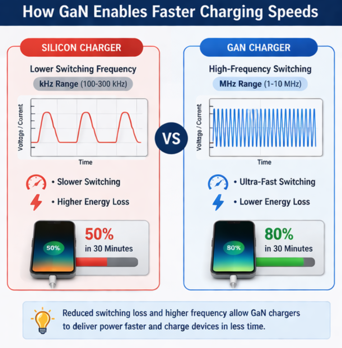
How GaN Enables Faster Charging Speeds
“GaN thrives where speed and power density matter most. Its ability to switch at MHz frequencies with minimal losses makes it ideal for applications where size and efficiency are critical.” — Microchip Technology Inc. Industry Analysis Team, Industry-leading semiconductor manufacturer and authority in power electronics
Switching frequency represents the heart of GaN’s charging advantage. While traditional chargers have made incremental improvements over the years, GaN technology brings a fundamental leap forward in how quickly our devices can recharge.
High-frequency switching in GaN transistors
The secret behind GaN’s impressive charging capabilities lies in its extraordinary switching speed. Silicon devices typically operate at switching frequencies limited to a few hundred kilohertz, whereas GaN devices function at several megahertz or even tens of megahertz. This dramatic difference emerges from GaN’s superior material properties.
At the transistor level, GaN devices can transition from on to off states in merely 1-2 nanoseconds, while silicon and silicon carbide transistors require 20-50 nanoseconds for the same operation. This ten-fold improvement in switching time directly translates to reduced switching losses. The switching process in GaN takes less than 7 nanoseconds, approximately ten times shorter than in standard MOSFETs.
This high-frequency operation enables several advantages:
- Smaller magnetic components (transformers, inductors)
- More compact capacitors
- Improved overall power conversion efficiency
- Reduced energy loss during charging cycles
Essentially, GaN’s rapid switching capability enables chargers to manage electricity more efficiently. One practical application involves DC-DC converters operating at switching frequencies of 100kHz and beyond, where GaN demonstrates substantially lower switching losses compared to silicon alternatives.
Reduced dead time and faster power delivery
“Dead time” represents a critical yet often overlooked factor in charger performance. It refers to the delay inserted between turning off one transistor and turning on another to prevent simultaneous conduction that would cause a short circuit.
Dead time directly impacts charging efficiency—the longer it lasts, the more energy gets wasted. GaN’s ultra-fast switching characteristics allow for significant dead time optimization. In high-frequency converters, minimizing dead time becomes increasingly important as operating frequency rises.
Laboratory tests demonstrate this impact clearly. In a 12V to 1.8V buck converter using an integrated GaN half-bridge device operating at 5 MHz, efficiency measurements with varying dead times showed a direct correlation between dead time length and power loss. Remarkably, small negative dead times even showed beneficial effects on efficiency before quickly degrading due to shoot-through.
For modern chargers, GaN’s ability to operate with minimal dead time translates to faster power delivery. Primarily, this means more energy reaches your device instead of being wasted as heat during switching transitions.
GaN vs Silicon in USB-C PD chargers
GaN’s advantages become particularly evident in USB-C Power Delivery (PD) chargers. These chargers support various fast charging protocols including PD3.0 and QC3.0, allowing devices to charge in a fraction of the time compared to conventional chargers.
USB-C PD chargers with GaN technology deliver multiple advantages:
- Higher power conversion efficiency: Converting power with less energy wasted as heat
- Faster charging: Operating at higher voltages and switching frequencies significantly reduces charging times
- Universal compatibility: Supporting a wider range of devices at their optimal charging rates
In direct comparisons, GaN chargers outperform silicon-based PD chargers in several key metrics. A GaN charger with 65W output can charge a typical smartphone to 50% in approximately 30 minutes and fully charge many laptops in under two hours. This speed advantage stems from GaN’s high conductivity, which translates to greater power conversion efficiency—often exceeding 90%.
Furthermore, GaN chargers support emerging standards like USB Power Delivery 3.0. The enhanced PPS (Programmable Power Supply) capability allows more granular voltage stepping, shifting heat generation from the phone’s power management IC to the charger, helping phones maintain higher charging currents without thermal throttling.
Indeed, GaN represents not merely an incremental improvement but a fundamental shift in charging technology, offering substantially faster charging speeds while maintaining cooler operation and smaller physical dimensions.
Compact Design: GaN’s Advantage in Power Density
Physical size matters tremendously for modern charging solutions. GaN technology offers an extraordinary advantage in this arena through its remarkable power density capabilities.
Higher power output in smaller form factor
The size reduction in GaN chargers stems directly from their inherent electrical properties. GaN power devices consistently achieve power density benchmarks exceeding 5,000 W/in³ compared to MOSFET-based converters at approximately 350 W/in³ before GaN adoption. This translates to a 14× improvement in power density—a monumental leap rather than an incremental change.
GaN’s higher electron mobility (over 1000 cm²/V·s versus silicon’s 400 cm²/V·s) allows electrons to move significantly faster through the semiconductor material. This superior electron transport directly enables smaller device dimensions without sacrificing performance. Practically speaking, GaN technology chargers can improve overall system efficiency by 10% while simultaneously shrinking the physical size by a factor of two compared to traditional silicon-based solutions.
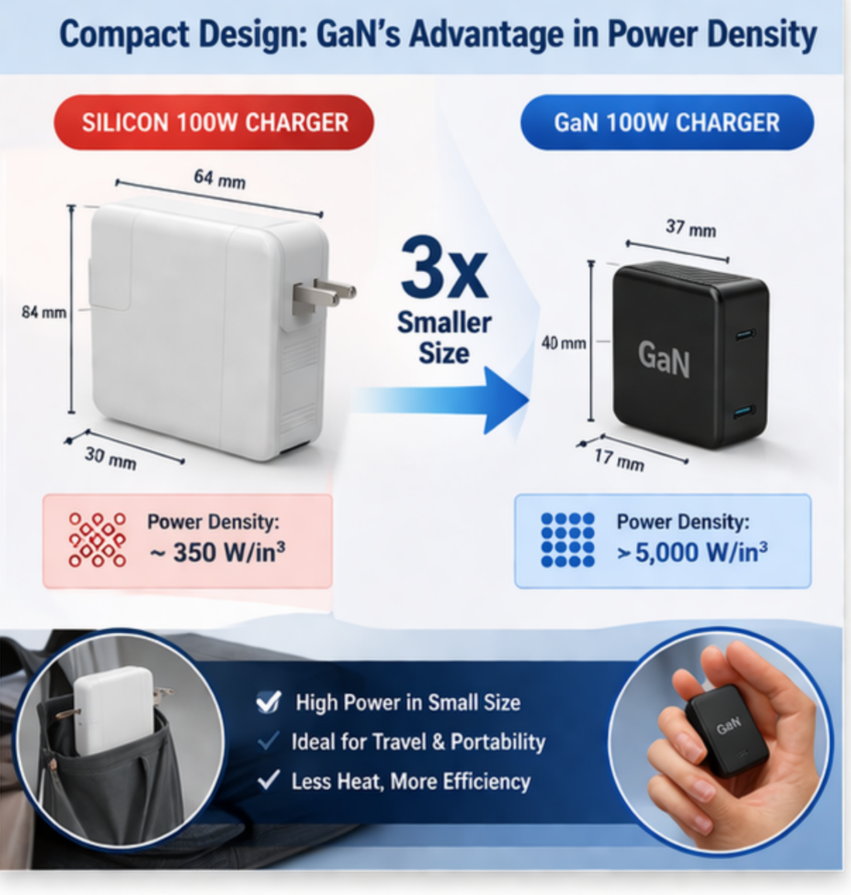
GaN’s role in miniaturizing 100W+ chargers
For high-power adapters, the difference becomes even more pronounced. Traditional 100W silicon chargers typically required bulky designs that made portability challenging. GaN-based alternatives have dramatically shifted this paradigm.
The fundamental advantage lies in GaN’s breakdown field strength—approximately 3.3 MV/cm compared to silicon’s 0.3 MV/cm. This tenfold improvement allows GaN devices to handle much higher voltages in significantly smaller spaces. Moreover, GaN’s ability to operate efficiently at higher frequencies enables the use of smaller passive components like capacitors and inductors.
These technical advantages manifest in practical terms: a typical 100W GaN charger occupies roughly one-third the volume of its silicon counterpart while delivering equivalent or superior performance.
Comparison of GaN vs Silicon charger sizes
The size difference between technologies becomes immediately apparent through direct comparisons:
- A 65W GaN charger can match the size of a standard 5W Apple iPhone charger
- 100W GaN adapters often match the dimensions of 30W silicon versions
- Multi-port GaN chargers can replace several individual silicon adapters while occupying less total space
Beyond raw size reduction, GaN chargers offer practical advantages in daily use. Their compact dimensions make them ideal for travel, fitting easily into pockets, purses or laptop bags. This portability factor represents a significant quality-of-life improvement for professionals and frequent travelers who previously needed to carry multiple bulky adapters.
Ultimately, GaN’s power density advantage creates a virtuous cycle—smaller components generate less heat, requiring less cooling infrastructure, further reducing overall size while maintaining reliability.
Durability and Long-Term Reliability of GaN Chargers
“GaN semiconductors can handle higher voltages and temperatures without degrading, making them last longer, particularly in environments where chargers are heavily used or need to handle more power.
GaN is inherently more robust under high-temperature and high-frequency operation.
Thermal stress resistance in GaN semiconductors
GaN devices excel under thermal pressure. These semiconductors can function effectively at temperatures reaching 200°C in power control units, outperforming traditional silicon-based alternatives. The thermal conductivity of GaN at room temperature measures 257 W/(m·K) for in-plane and 275 W/(m·K) for cross-plane directions, enabling superior heat dissipation across challenging conditions.
Although thermal stress affects all electronic components, GaN’s material properties make it exceptionally resistant to degradation. This resistance comes from its ability to withstand both the mechanical stresses and electrical fluctuations that typically damage silicon chargers over time.
This improves reliability in:
- Continuous high-load operation
- High ambient temperature environments
- Industrial power applications
- Lower Failure Rates in Real Use
GaN’s performance in high-usage environments
In real-world applications, GaN technology has demonstrated impressive durability. Since entering volume production in 2010, eGaN devices have established an outstanding field reliability record. Their exceptional performance under stress has been confirmed through extensive testing protocols specifically designed for GaN power devices.
For users who frequently charge multiple devices, this translates to consistent performance without the degradation common in silicon chargers. High-quality GaN adapters maintain stable operation even in demanding environments characterized by temperature fluctuations and continuous usage.
Failure rate comparison: GaN vs Silicon
The longevity difference between technologies is substantial. Well-manufactured GaN chargers typically last between 5-10 years under normal usage conditions, versus only 2-5 years for traditional silicon-based alternatives. This extended lifespan stems from GaN’s superior efficiency and reduced heat generation.
GaN’s reliability metrics now match silicon’s established standards, yet with significant advantages in thermal performance. Major manufacturers have documented this reliability through accelerated testing, with results indicating that GaN devices can exceed 10 years of operational life.
This makes GaN particularly suitable for OEM and industrial-grade power designs.
Environmental and Cost Benefits Over Time
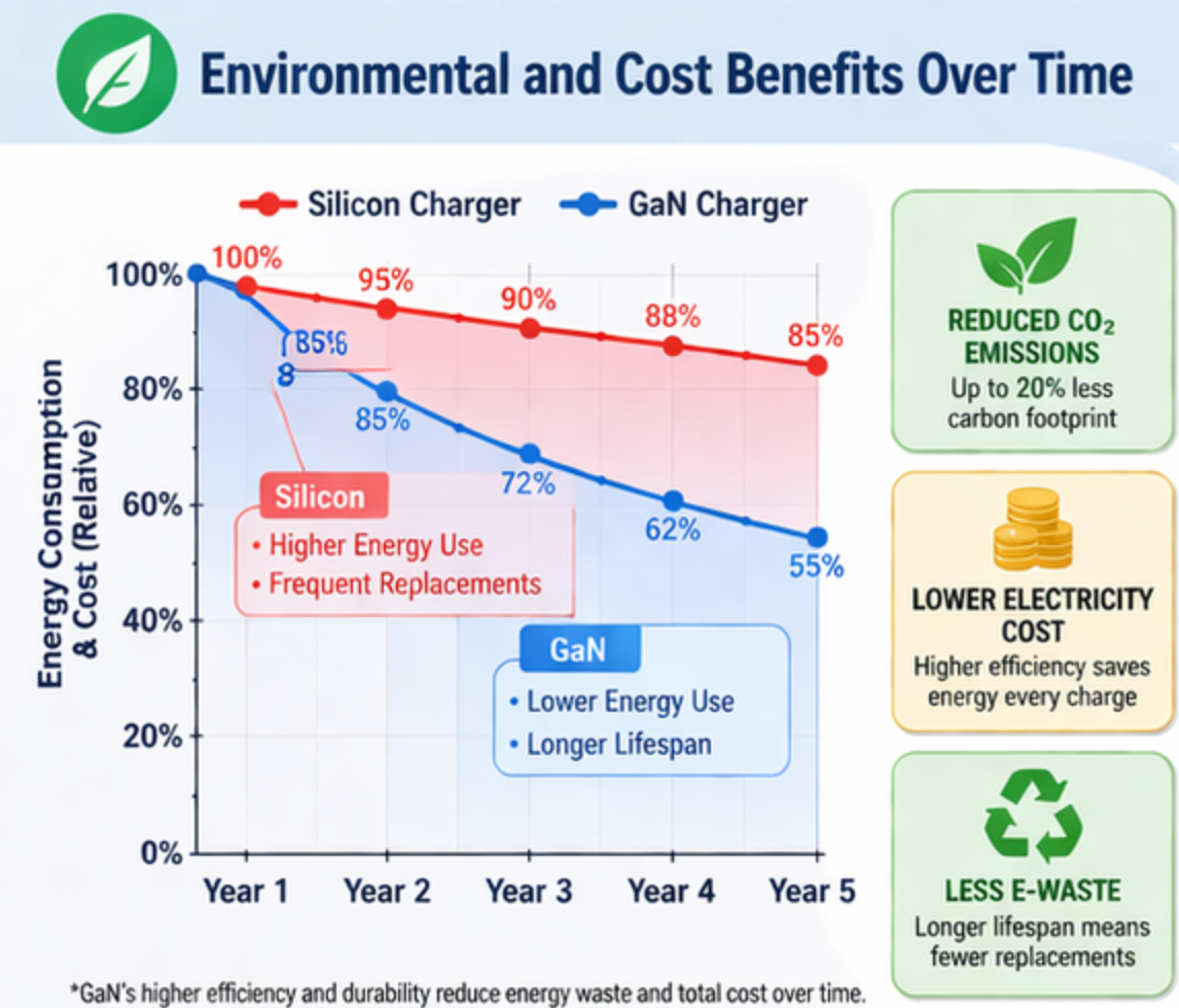
Beyond performance advantages, GaN technology offers substantial environmental and economic benefits that continue to strengthen its value proposition.
Lower energy waste during charging cycles
First and foremost, GaN chargers demonstrate remarkable efficiency advantages over traditional silicon options. With energy conversion efficiency exceeding 90% compared to silicon’s 80-85% range, GaN technology wastes significantly less power during each charging session. This efficiency differential translates directly into reduced electricity consumption.
According to industry measurements, a typical GaN charger operates at 95% efficiency versus just 87% for silicon-based alternatives. Over time, this difference adds up—especially for frequent device users. Given these points, replacing all silicon chargers with GaN technology could potentially reduce global consumer energy usage by 10-20%.
Material efficiency and reduced e-waste
The compact design of GaN chargers—approximately 40% smaller than silicon equivalents—directly contributes to material conservation. This size reduction means fewer raw materials in manufacturing and less packaging waste.
Despite initially appearing as a minor advantage, this material efficiency combines with GaN’s extended lifespan to create substantial e-waste reduction. Under those circumstances, GaN chargers typically last 5-10 years compared to silicon’s 2-5 year average, effectively halving electronic waste generation from chargers.
Price trends: GaN vs Silicon over the next 5 years
Until now, GaN chargers have carried premium pricing due to newer technology and manufacturing processes. Nevertheless, the market is evolving rapidly with a projected 49% CAGR between 2022 and 2028.
The price gap continues narrowing as production scales up. In the long run, ongoing innovations in manufacturing—particularly the shift to 8-inch wafers—are reducing production costs by 30-40%. For this reason, many current GaN devices already achieve price parity with comparable silicon alternatives.
Real-World Applications of GaN Chargers
GaN technology is widely used in:
- USB-C fast chargers (45W–140W)
- Laptop power adapters
- Multi-port charging hubs
- LED display power systems
- Networking and communication equipment
- Industrial embedded power systems
Its ability to deliver high power in compact form makes it ideal for both consumer and industrial applications. Learn more about the apllications of GaN Charger.
Explore our full range of GaN power adapters designed for USB-C PD, industrial, and OEM applications.
When Should You Choose GaN Chargers?
GaN chargers are especially suitable when:
- Portability is important
- High power output is required in small size
- Heat dissipation is a concern
- Multi-device charging is needed
- Efficiency and long-term reliability matter
For high-performance applications, GaN is increasingly becoming the default choice.
If you already understand the differences between GaN and silicon chargers, the next step is choosing the right 100W GaN charger for your specific application. To help you avoid common mistakes and select the most suitable model, we’ve prepared a detailed selection guide.
👉 Read next: How to Choose a 100W GaN Charger: Key Specs, Safety & Compatibility Guide
FAQ: GaN vs Silicon Chargers
What is the main advantage of GaN over silicon?
Higher efficiency, lower heat generation, and significantly smaller size.
Are GaN chargers faster?
Yes. Higher switching frequency and better efficiency enable faster and more stable charging performance.
Are GaN chargers worth it?
Yes, especially for high-power or portable use cases, due to better efficiency and longer lifespan.
Do GaN chargers last longer?
Yes. Lower thermal stress typically results in longer operational lifespan than silicon-based chargers.
Conclusion
GaN technology represents a fundamental improvement over traditional silicon-based power adapters. By enabling higher switching speeds, lower heat generation, and significantly higher power density, GaN chargers deliver superior performance in nearly every key metric.
Compared to silicon chargers, GaN provides:
- Higher efficiency
- Smaller size
- Lower operating temperature
- Longer lifespan
- Better overall energy utilization
For modern electronics requiring fast, efficient, and compact power delivery, GaN is no longer an alternative—it is becoming the standard.